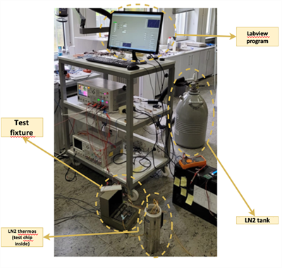
Down-scaling of transistor sizes continues unprecedently with the device channel lengths approaching closely to atomic dimensions. This progress leads to a great degree of process variations, which complicates the analog or digital circuit design since it gets harder to achieve the design specifications. In addition to these challenges, time-based degradation of transistors or extreme environmental conditions such as cryogenic temperatures or ionizing degradation also modify the current-voltage characteristics of solid-state electronic devices. Hence, developing a transistor model that can account for all these conditions and be applied in different circuit design applications becomes a major challenge. Assoc. Prof. Dr. Mustafa Berke Yelten, from Istanbul Technical University Electronics and Communications Engineering, and his research team work towards building a "holistic transistor model" that can accommodate the process variations and reliability degradations as well as extreme conditions. Experimental characterization of the designed test chip at 40 nm bulk CMOS technology is ongoing in ITU VLSI Laboratory. Initial results suggest that combinations of different operating conditions can lead to distinct outcomes that can only be anticipated if a "holistic" device model is employed during circuit simulations.
X. Xhafa, A. D. Güngördü, D. Erol, Y. Yavuz and M. B. Yelten, "An Automated Setup for the Characterization of Time-Based Degradation Effects Including the Process Variability in 40-nm CMOS Transistors," in IEEE Transactions on Instrumentation and Measurement, vol. 70, pp. 1-10, 2021, Art no. 2005110, DOI: 10.1109/TIM.2021.3090175.

